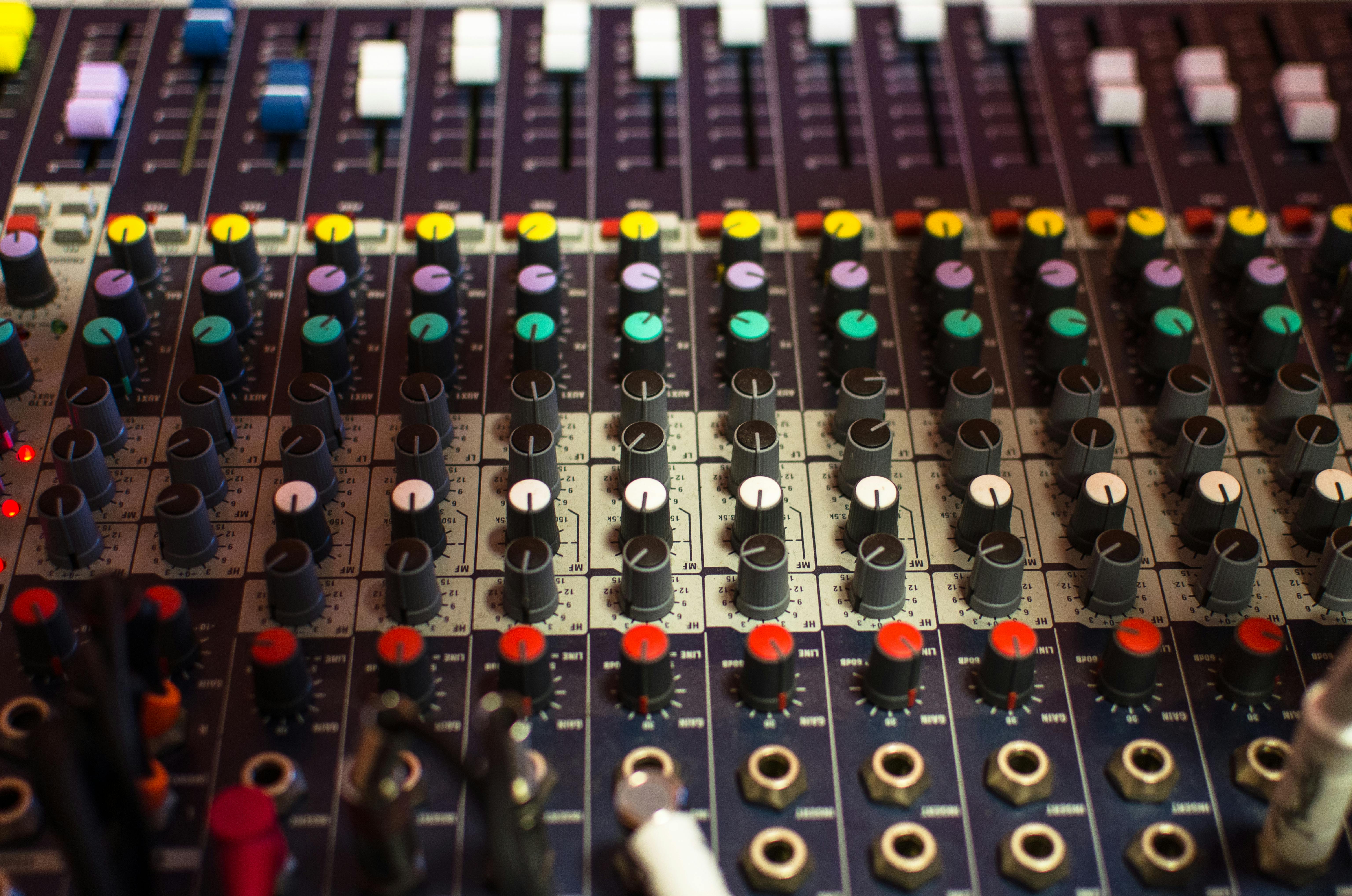
Durability of RF PCB Design
The modern world relies on a wide range of RF (Radio Frequency) PCBs for communication systems, radar equipment, satellite technology and countless other applications. These tiny yet highly complex circuit boards transfer and dissipate current that powers the devices we use every day. To function properly, these circuit boards must deliver signal transmission, reception and stability with minimal interference from external sources. This can be achieved with careful RF pcb design, including the proper placement of components and the utilization of specific PCB materials to avoid signal loss and other issues.
Some of the main factors influencing the durability of rf pcb design are signal losses, cross-talk and other unintentional electromagnetic interference. These interferences are caused by the alternating current flowing across the surface of the conductor, which creates skin effect, increasing resistance and reducing effective impedance. In addition, high-frequency signals have a tendency to couple with closely spaced other traces and components, resulting in unwanted data corruption or signal attenuation. This can lead to an increase in the overall power consumption of a circuit board or the need for more complex signal routing to mitigate the issue.
RF PCBs are usually multi-layered to optimize their performance, and each layer must have precise characteristics for the intended application. For example, rf pcb design require substrates that can handle the high-frequency operation and exhibit a consistent dielectric constant, loss tangent, and coefficient of thermal expansion over a broad frequency range. They also need to be durable and inexpensive to minimize manufacturing costs.

The Main Factors Influencing the Durability of RF PCB Design
The PCB stack-up, the arrangement of layers and their thickness, is another important aspect of RF pcb design. This includes the use of signal, ground and power planes to provide shielding, reduce sheet resistance and improve decoupling between signal and non-signal layers. It is also critical to ensure the correct insertion of through-hole and surface mount components, as well as avoiding any overlap between layers.
Impedance matching is also essential for RF pcbs, as it allows signals to travel longer distances while minimizing their reflection and transmission losses. This is achieved by using the correct trace width and characteristic impedance to match the impedance of the RF components.
A good RF design will also include ground vias between each layer of the board, ensuring that they remain close to the signal layers and preventing the accrual of parasitic ground inductance. This prevents the transmission of interference from the RF signal to the rest of the circuit and reduces the chances for electronic failure.
The specialized RF design process begins with a detailed schematic and ends with a physical prototype. This prototype is used to test the performance of the RF circuit board before it can be manufactured in bulk. During the prototyping phase, it is vital to use a reliable platform that enables RF PCB designers to make changes quickly and easily. With Altium 365, engineers can quickly share their designs with their manufacturers and track the fabrication process, all without needing to send emails or use external chat programs.